Crowdly
Add to Chrome
ECE3161 Analogue Electronics - MUM S2 2025
Looking for ECE3161 Analogue Electronics - MUM S2 2025 test answers and solutions? Browse our comprehensive collection of verified answers for ECE3161 Analogue Electronics - MUM S2 2025 at learning.monash.edu.
Get instant access to accurate answers and detailed explanations for your course questions. Our community-driven platform helps students succeed!
Q10. Find component values to make the transfer function frequency independent
The filter given below has the transfer function T(s)= v_{out}(s)/v_{in}(s) where
s is the Laplace variable. If
C_1 \neq C_2, and
R_1 \neq R_2, given
C_1,
R_1, find
C_2, and
R_2, if gain is frequency independent and equal to
-G where
G is a real positive number.
0%
0%
0%
0%
0%
View this question
Q10. Determine the small signal differential gainWhat is the small signal differential gain  v_{od}/v_{id} for the differential pair below at temperature 300K. Assume both transistor are identical.
0%
0%
0%
0%
0%
View this question
Q9. Determine the resistor valueFor the circuit given below, determine the resistor value  R that gives a small signal differential
  v_{od}/v_{id} equal to 50 at temperature 300K. Note that all the PNP transistors are identical and have an Early voltage of 4V. All the NPN transistor are identical and have an Early voltage of 5V. Hint: when tackling this problem, remember detailed small signal model is needed only for NPN transistors as PNP transistors provides biasing. So, their dynamic resistance based on Early voltage is the only thing matters for calculations.
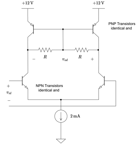
0%
0%
0%
100%
0%
View this question
Q7. Determine the small signal differential gainFor the differential pair below, find the small signal differential gain  v_{od}/v_{id} at temperature 300K. Assume both transistor are identical and have an early voltage of 5V.
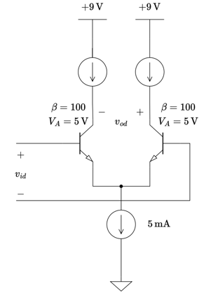
❌
❌
❌
❌
✅
View this question
Q8. Determine the minimum supply voltageA common mode voltage of 1V is applied to the NMOS differential pair below. Assuming both NMOS transistors are identical and their threshold voltage  V_t=0.5\text{V}, what is the minimum allowable power supply voltage
  V_{DD} if both transistors to remain in saturation?
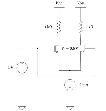
❌
❌
✅
❌
❌
View this question
Q5. Find the collector voltageFor the differential pair below, both NMOS are identical and both NPN are identical. What is the collector voltage  V_c?
V_c?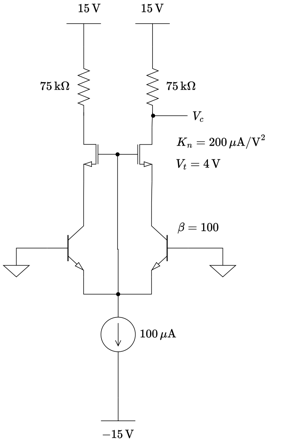
100%
0%
0%
0%
0%
View this question
Q6. Find the bias current What is the bias current  I_E of the differential pair at temperature 300K. Assume both transistor are identical.
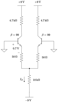
0%
0%
0%
0%
100%
View this question
Q4. Determine the small signal differential gainWhat is the small signal differential gain  v_{od}/v_{id} for the differential pair below at temperature 300K. Assume both transistor are identical.
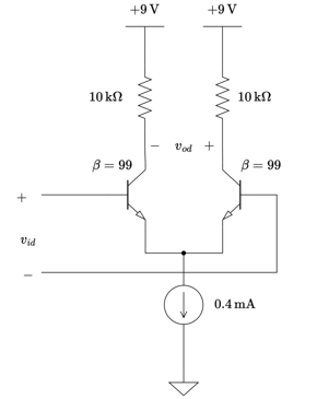
0%
100%
0%
0%
0%
View this question
Q3. Determine the collector voltageFor the circuit given below, determine the voltage  V_c. Assume all transistors are identical and their
  V_{be}=0.7\text{V},
  \beta = \infty.
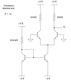
0%
0%
0%
0%
0%
View this question
Q2. Determine the CMMR in dBA certain differential amplifier has a differential gain  Ad=2000 and common mode gain
  Ac=0.2. What is the CMMR in dB?
0%
0%
0%
0%
0%
View this question